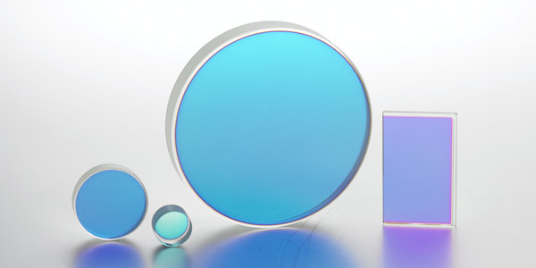
Smart optics
Our optics are used in lasers, measurement instruments, telescopes, on satellites, or in lighting systems. To open up new applications in the future, we work on smart optics by optimizing layer precision, minimizing losses, increasing homogeneity over a larger area, and by improving power compatibility. We are also developing fiber optic components for new laser applications and for the miniaturization and integration of optics.
Your contact person
Dr. rer. nat. Andreas Wienke

Follow us

Overview of smart optics
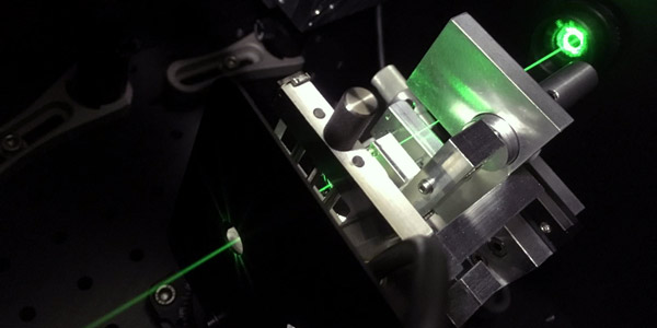
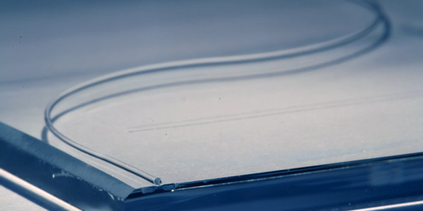
Fiber optic components
With smart fiber components also for special fibers, we develop monolithic and thus alignment-free fiber lasers and amplifiers. Using our specialised, internally developed plants, we are able to manufacture highly integrated fiber systems with all the necessary optical behaviour. For instance fiber-based coupling, decoupling or modifying of optical laser radiation. This unique combination of special fibers and highly integrated fiber components with special fibers enables customized fiber lasers and amplifier systems for new application areas.
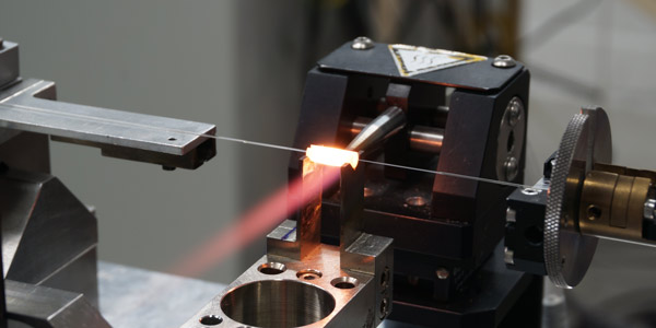
For the production of fiber components, we rely on plasma, hydrogen flame, or laser-based manufacturing processes. We use these to laterally weld fibers together (splicing), taper the fibers, or microstructure them. Laser-based methods make it possible to avoid contamination of the fiber components and to automate the process. We are currently researching and developing automated manufacturing processes using CO2 and CO lasers.
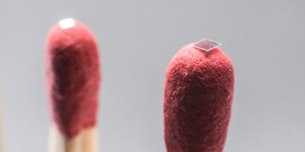
End caps, cladding light strippers, mode field adapters, pump combiners, or wavelength division multiplexers - we develop components for fiber lasers that optimally meet individual customer requirements. In particular, we use special fibers such as PCF (photonic crystal fibers) or CCC fibers (chirally-coupled-core) to be included as standard in integrated fiber links in the future. In addition, we investigate the integration of how hollow-core fibers into fiber components to transport single-frequency high-power signals or ultrashort pulses. We can weld several output fibers of laser systems to an end cap, combine their output powers, and thus precisely control the intensity profile of the laser radiation, for example in material processing.
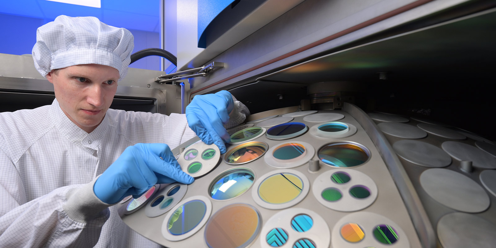
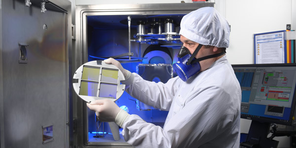
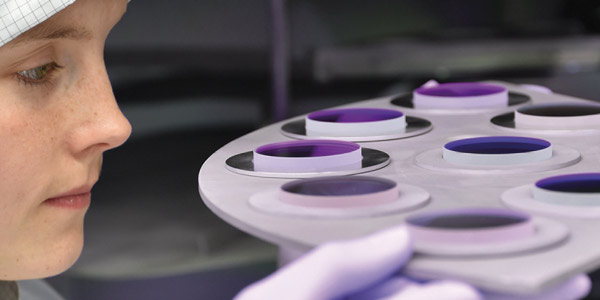
Optical coatings
From the short-wavelength ultraviolet (UV) range to the long-wavelength infrared (IR) range: we develop smart optical coatings perfectly tailored to the planned application and optimized for long life service. We develop coating systems that are not commercially available, work on spectral broadband monitoring, and open up new coating methods and dimensions to enable new applications with our optics and equipment.
We develop processes for various coating methods individually tailored to the planned application. In doing so, we test the limits of what is possible and develop sophisticated methods for innovative coatings from the short-wave UV range < 200 nm to the long-wave IR range > 6 µm. We work with various oxide and fluoride materials and optimize their absorption and refractive index for the specific application. We use the following processes:
• Ion Beam Sputtering (IBS)
• Atomic Layer Deposition (ALD)
• Electron beam coacting (E-Beam)
• Magnetron Sputtering
• Ion assisted deposition (IAD)
• Molecular-beam Epitaxy (MBE)
To characterize optical components, we use a wide range of measurement methods and develop them further. We also collaborate in the development of standards and ISO norms. Our current spectrum:
- Laser-induced damage thresholds (LIDT)
- Laser Calorimetric Absorption (LCA)
- Cavity Ring Down (CRD)
- Spectrophotometry (UV - IR)
- Scattered light measurements
- Interferometry
- Durability and environmental tests
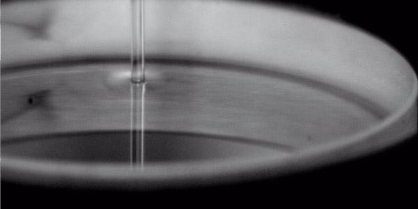
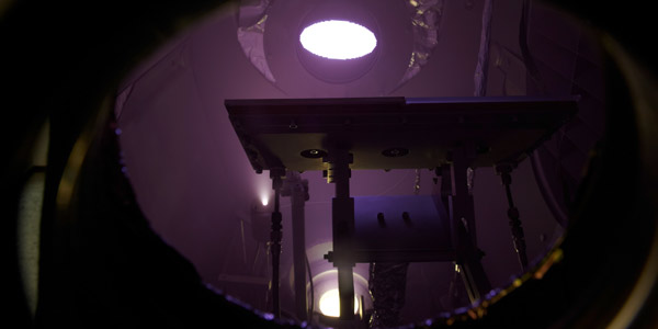
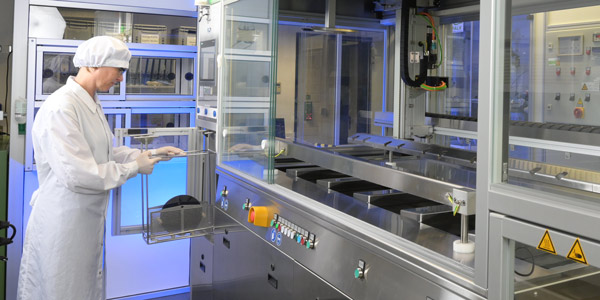
We use our expertise in a wide range of coating processes to continuously optimize existing processes. With the development of novel adaptive shadow masks, we adapt equipment precisely to the materials and substrates used in coating processes. We meet the highest homogeneity requirements for our coatings of < 0.1% on radii up to 200 mm through usage of shadowing masks and planetary gears. We ensure highly efficient, precise, and reliable coating processes by integrating in-situ measurement technology for spectral broadband monitoring. Our broadband monitor BBM can also be developed with multiple measurement radii, wavelength ranges and resolutions, and different operating modes (reflection or transmission). Furthermore, we investigate scalable methods for fiber end face coating by novel system concepts.
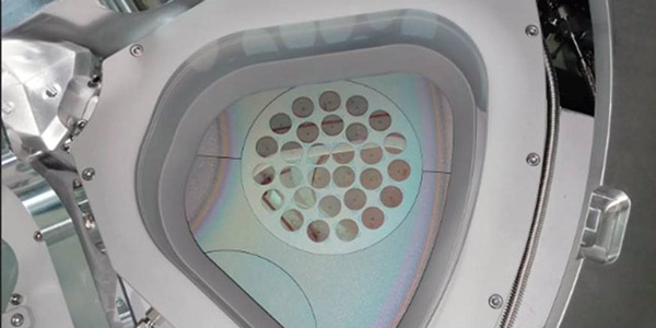
Atomic layer deposition is little established for optical coatings. Still, it is superior to other coating processes in terms of uniformity and flexibility. With the so-called Spatial ALD process, we can increase the coating speed with better uniformity. Furthermore, we want to use the process to efficiently produce high-quality coatings on structured or free-form surfaces in the future, which is not possible or only insufficiently possible with traditional coating processes. We are also working on coating 3D-printed plastic components in the low-temperature range (<120°C), thus providing them with optical functions or protective coatings against environmental influences.
Optical materials
Understanding optical materials is the basis for developing smart coating processes, intelligent monitoring, and new system technology. We use simulations to adapt real processes as early as possible, optimize the coating design for the planned application and exploit nonlinear interaction processes to equip coatings with novel functions. With quantum nanolaminate structures, we are advancing into new application areas.
Simulations help us to better understand coating processes and enable us to gain new process knowledge that we transfer to the application with simulations. Particularly in the case of complex coatings, we carry out virtual process simulations in advance to adapt the real processes accordingly. We simulate the coating synthesis to determine properties in advance and select the coating parameters in the best possible way for the application. In addition, we use simulation methods to explore the behavior of new optical materials, and can thus bring them into practice more quickly.
To adapt optical material properties to individual requirements, we can optimize the refractive index and band edge of the materials independently using a special process. We achieve this by creating so-called quantum nanolaminate structures, which change the electron structure of the highly refractive material embedded in the layer system. On the one hand, this allows us to produce better coating systems for the UV range and, on the other hand, to optimize the damage threshold of the coating system.
Coatings are subject to different stresses and requirements depending on the area of application. Therefore, we are primarily working on power resistance and long-life operation. We optimize coating structures to actively counteract damage, make coatings more robust and to reduce internal stress, which in turn increases the optics durability. In particular, we are working to maximize laser-induced damage thresholds (LIDT) of optics and optical coatings from the CW to the femtosecond range. This enables the development of more powerful high-power lasers for the industry. To this end, we are working on reducing substrate degradation effects, enabling more durable optics, and opening up new substrates materials.

With active layers, we can create optical components with complex functions. We use nonlinear interaction processes of the incident laser light with the layer material to realize fast optical switches. This makes it possible, for example, to influence the mirror function in transmission and reflection with an intense switching pulse. To make the switching of light in optical layers with total thicknesses of less than micrometers possible in principle, we use nonlinear material properties that we continuously optimize to lower the switching thresholds and enable other functionalities. In the process, we have already succeeded in integrating frequency conversion into mirror layers and generating the third harmonic of the incident laser light.
Optical components
Complex coating systems targeting the highest challenges and new solutions for the design of optical systems - we develop the optical components of tomorrow. This is made possible by our decades of experience and our future-oriented thinking.
We develop complex coating systems for special applications, such as lasers, telescopes, or other astronomical devices on earth and in space. In doing so, we dedicate ourselves to challenges beyond commercially available systems and research to push the limits of what is possible. Amongst others, we develop filter systems for fiber optics or high-quality anti-reflective coatings in the mid-infrared range, for example for thermographic cameras.
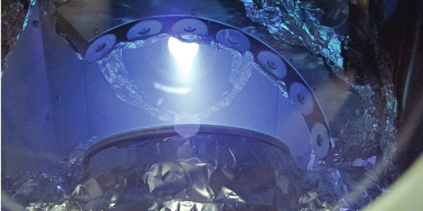
Large-area coatings are interesting for high-resolution telescopes, for example. We reliably coat substrates up to 0.5 meters and are currently even expanding this to a globally unique 2-meter diameter with ion beam sputtering. For this purpose, we ensure a uniform coating thickness over the entire coating area. Together with partners from small and medium-sized companies, we are developing adaptive uniformity screens for this purpose. These are intended to flexibly compensate for fluctuations in drifting processes. We will also use this approach to anneal differently shaped objects in one coating process.
Optical systems still consist of a multitude of discrete optical elements in complex optomechanical assemblies. Both optomechanics and functional optics can be rethought through innovative design approaches and the advantages of additive manufacturing. For example, we are working on individualized manufacturing of tailored GRIN lenses and waveguides made of glass and polymer, which can be integrated into chip-based microphotonics. We are also working on strategies for stress-free imprinting of (thermally active) optical components for highly integrated laser and multi-material systems. In this way, we can significantly save material and weight and thus manufacture compact, optical systems in a more sustainable and, at the same time, more cost-efficient way.
Miniaturization & integration
The miniaturization and integration of optical elements enable the production of complex optoelectronic assemblies and systems for application in communication, sensor technology, and quantum technologies. We develop new concepts for optical filters, which can even have adjustable properties. Intelligent concepts for the assembly of further optical components make it possible to realize optoelectronic systems in the smallest possible space.
Miniaturized optical filters are of particular interest for tele- and data communications. In the future, they will be integrated in even smaller spaces and exhibit lower optical losses. Therefore, we work on self-supporting and stress-free coating systems that cover a wide spectral range. We have successfully developed a special process for the production and transfer of substrate-free coatings. Furthermore, we are working on coating strategies to manufacture different filter specifications, which are specifically created in only one single pass of the coating process.
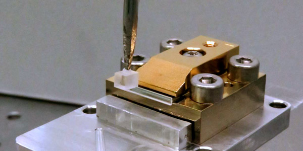
For optical systems in the smallest of spaces, particularly precise assembly is a prerequisite. We work on optoelectronic components' passive and active alignment and understand their electrical and mechanical contacting (die bonding). We also work on solutions for self-aligned assembly, for example by intelligent processes that do not require any further positioning driven by electrostatic forces or surface tension. We use flip-chip assembly for contacting unhoused semiconductor chips or for upright assembly of miniaturized optical components to increase the integration density in assemblies.
Optical metrology
The fundamental spectral properties of optical coatings must be measured much more precisely and extensively for future requirements than is possible with current instruments on the market. The established spectrophotometers, for example, are designed for other industries and no longer meet the constantly increasing demands of smart applications. For this reason, we at LZH are working together with companies on new, customized measurement systems for optical coatings.
As the demands on optical components increase, we design and build measurement devices that keep pace with this development. Among other things, we work on:
- Spectrophotometers (VUV-VIS-IR) for the determination of spectral transfer functions
- Broadband monitor systems for layer thickness determination and process optimization of optical coatings
- Laser calorimetry (VUV-IR) for high-precision absorption measurement
- LIDT measuring stations for determining the laser damage threshold of optics
- Scattered light measuring stations for mapping scattering sources, e.g. particles and surface roughnesses
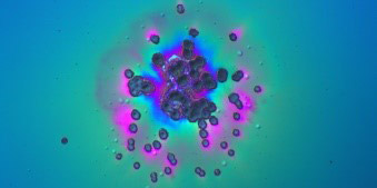
To reduce the effects of contamination or other damage in optical coatings, we work to minimize the particle load of optics before and during the coating process using laser and ion-assisted processes. In doing so, we focus on detecting and removing particles in time. Since particles can be the starting point for damage to optics during operation, our coatings are significantly more resistant due to these optimizations.
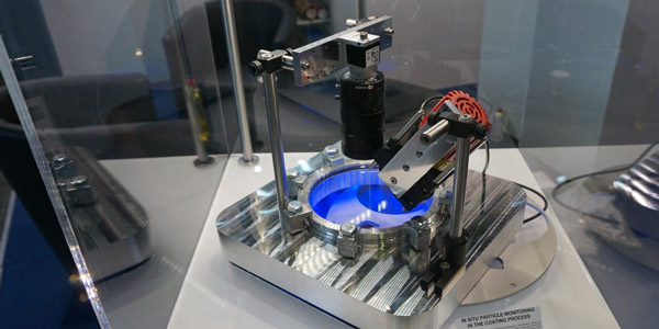
During an ongoing coating process, in-process analysis allows it to be controlled at an early stage or, even better, to intervene in a regulating manner. Therefore, we develop intelligent analysis methods that monitor various aspects of the coating process in real-time:
- Particle monitoring for the detection of particles and impurities on optics
- Plasma monitoring to measure properties, e.g. energy or composition of plasmas in coating and etching processes
- Spectral analysis to determine coating thickness or composition
- Layer stress analysis for monitoring the deformation of optics by the coating material
Coating processes are generally time-consuming, machine-intensive, and therefore expensive. Even small errors in the process can have a fatal effect on the properties of the coating. Our high-resolution broadband monitoring system (BBM) detects such errors and, with the help of smart software control, automatically adjusts further process steps to the target design. This technology enables significantly better and more reproducible manufacturing of optical coatings. Currently, we further develop the system to also capture special phase information of the mirror coating live by spectral phase control. This is essential, for example, for the production of chirped mirrors for the development of novel femtosecond lasers.